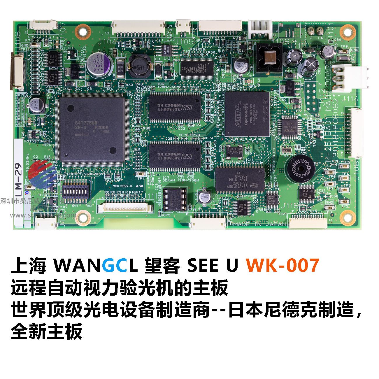
望客的SEEU是一个自动视光机,能读取用户眼镜的数据, 并进行虚拟试戴帮助用户快速做出最适合自己的选择眼镜。SEEU还可以直接读取用户眼睛的数据帮助用户进行验光并将数据推送给眼科医院,进行眼睛健康的远程诊断。
“SeeU自助视光机器人”,望客与世界顶级光电设备制造商日本尼德克共同研发制造的验光机器人,让用户便捷、自由地获取配镜处方。“SeeU自助视光机器人”1.0版,将在学校、社区、商圈、图书馆、餐厅等场所安装,可帮助眼镜佩戴人群免费自助获取精准配镜处方,为用户解决配镜必须去医院、传统眼镜店排队验光的麻烦,将专业验光带入寻常百姓生活,让用户轻松体验网络配镜。“SeeU自助视光机器人”2.0版,可帮助用户获取眼睛的“眼球分析影像报告”,帮助用户免费进行视力检查,获悉眼部健康档案,从而让用户更深度了解自己眼部健康方案,以及定制隐形眼镜、功能型光学镜的验配方案。
在既要保证低价,又要节省开店成本的前提下,望客创始人彭永泽从原本必须在线下完成的验、选环节入手,研发出自助验光机(See U)和基于AR技术的试戴App(See Me),并运用工业4.0先进制造理念创建了自动化交付中心。在望客的商业逻辑中,See U替代了传统门店,成为线下触达用户的渠道,可以说望客采取的是一种非常规的O2O模式。为了将See U更多地布局到消费者身边,望客目前通过三大渠道进行布点:一是国家体育总局的体育场馆,二是国家卫计委的医院和校医院,三是加盟商。按照望客的规划,在未来,无论是学生、上班族或是普通市民,都可以方便地在学校、医院、商务中心、地铁站或社区,通过See U自助验光,并轻松完成配镜流程。
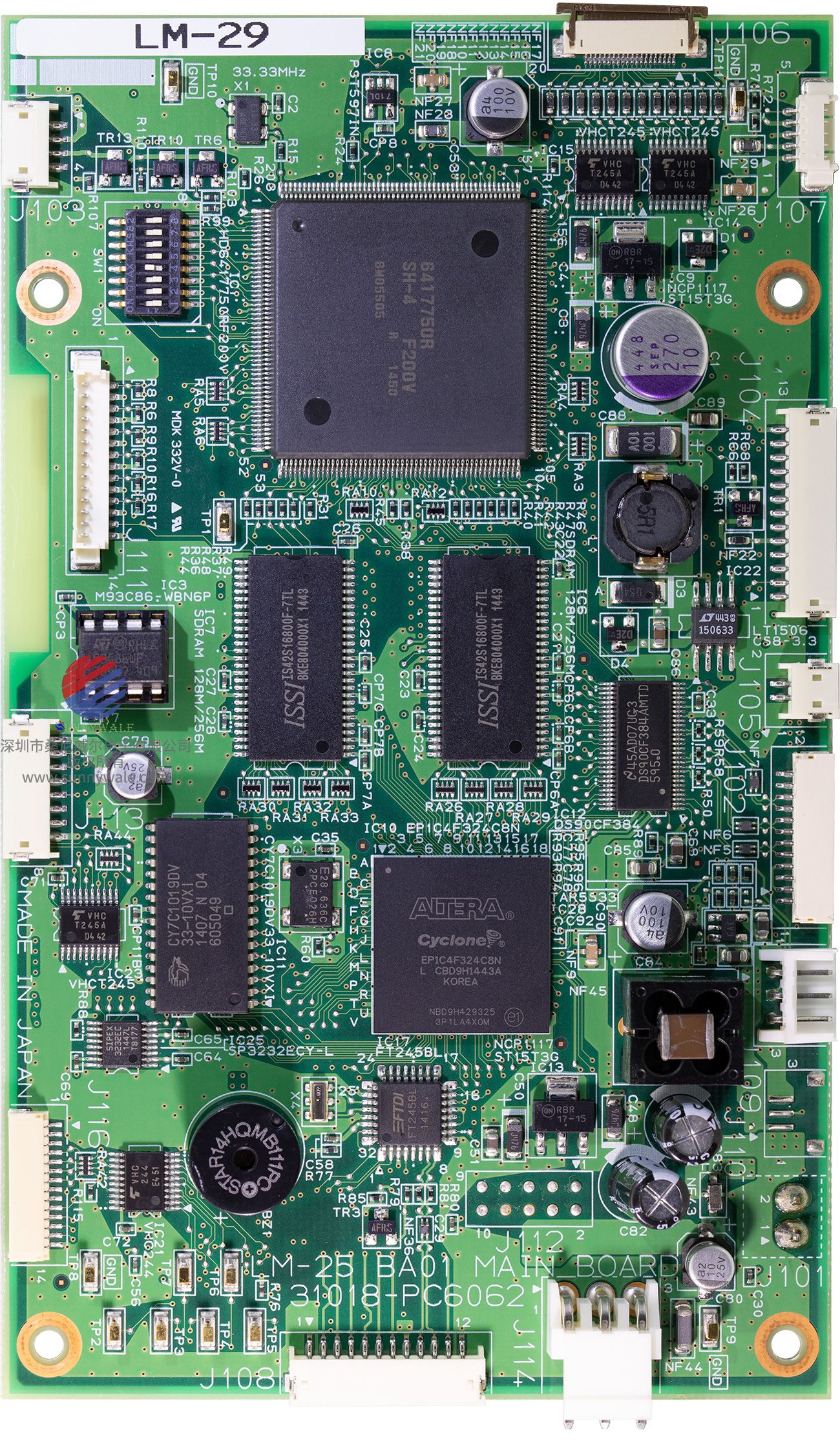
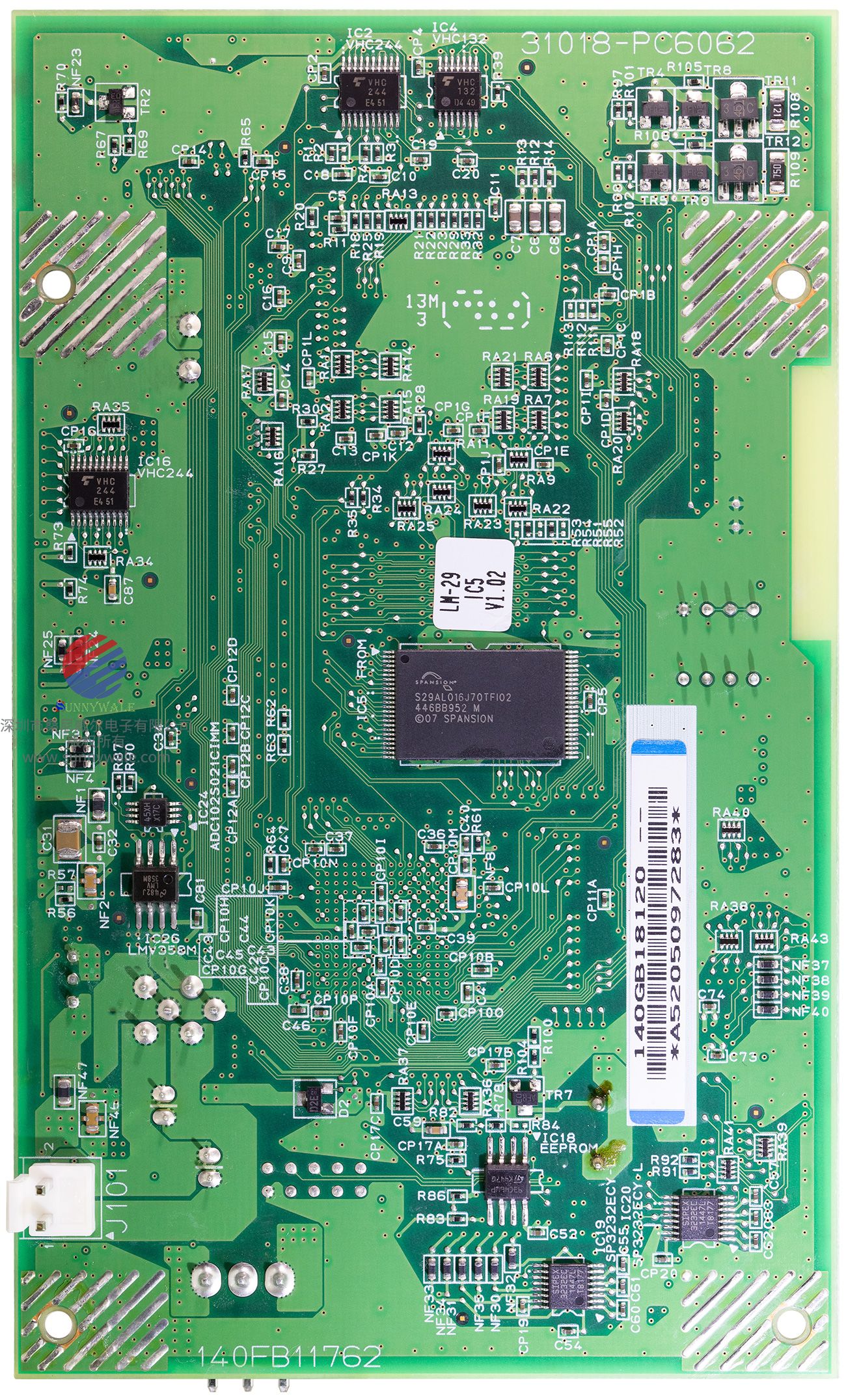
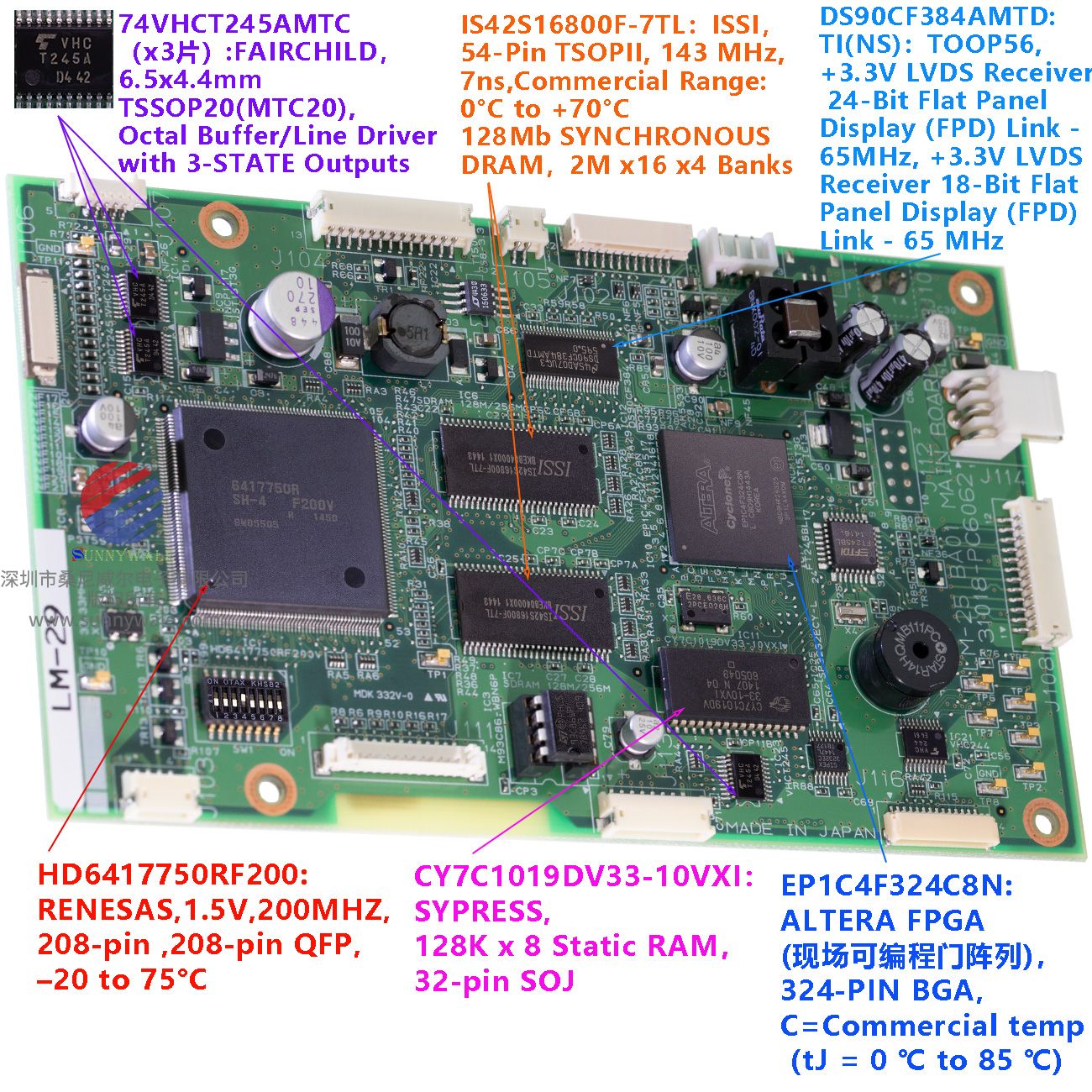
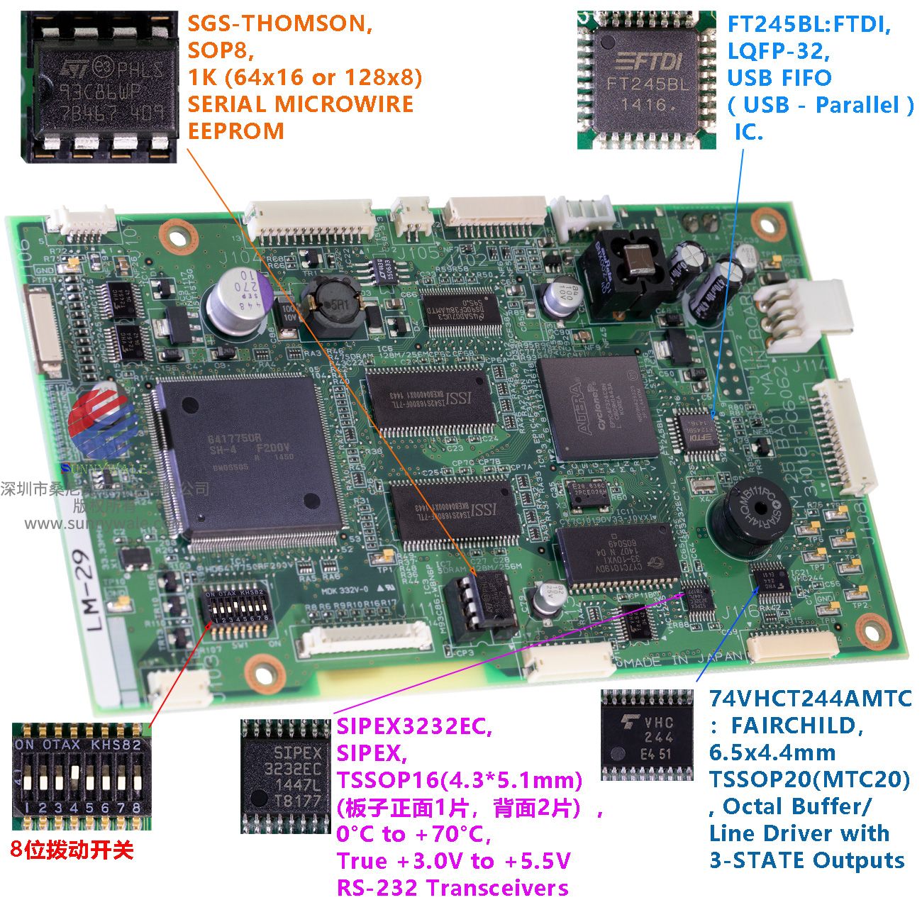
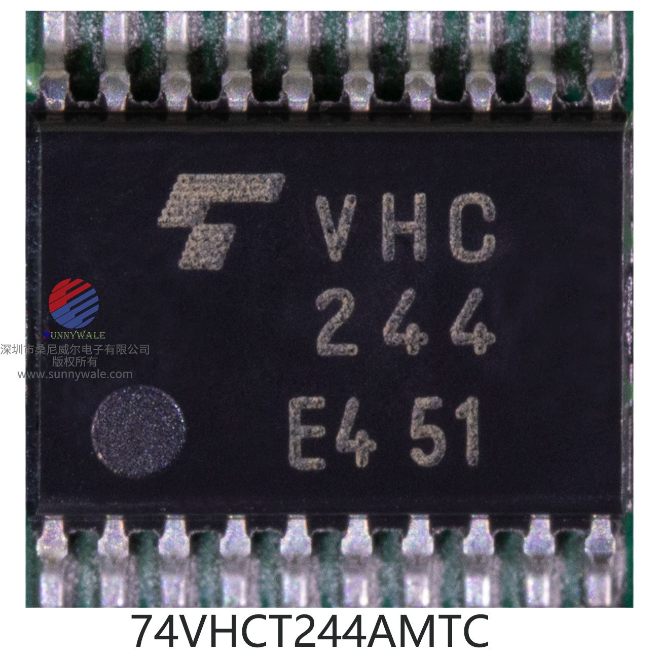
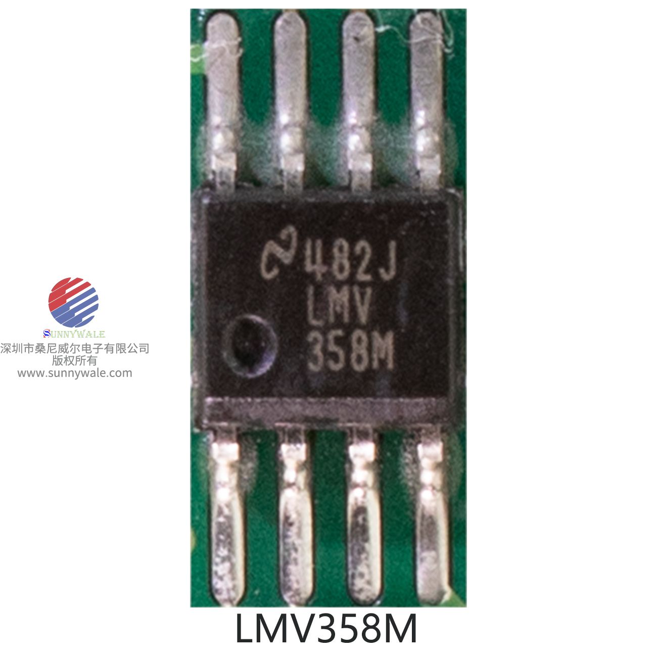
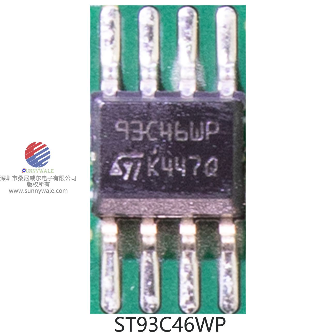
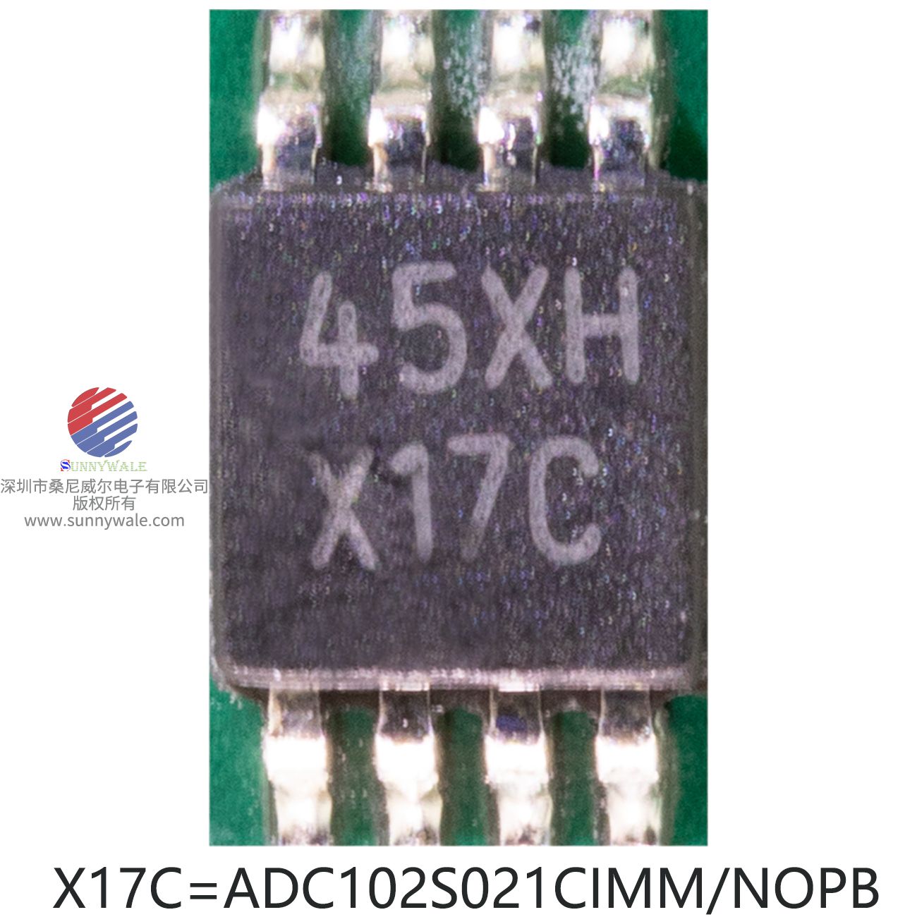
正面板载IC:点击相应的蓝色感应区,可免费下载 datasheet PDF(蓝色链接)
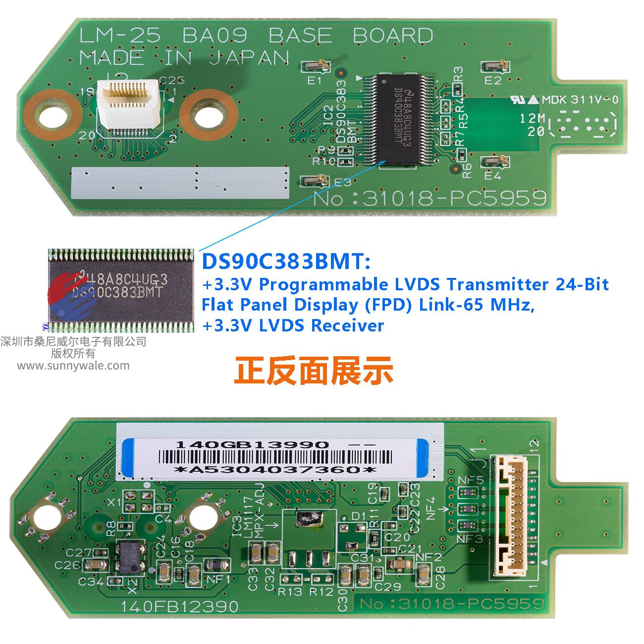
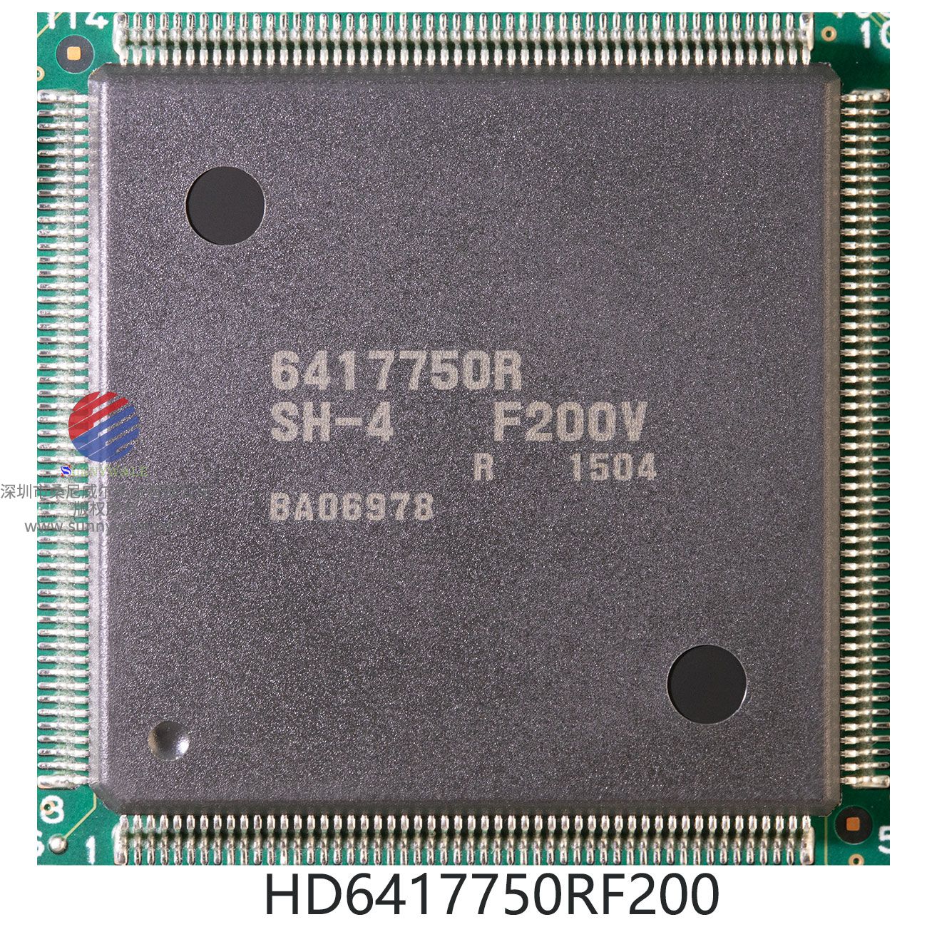
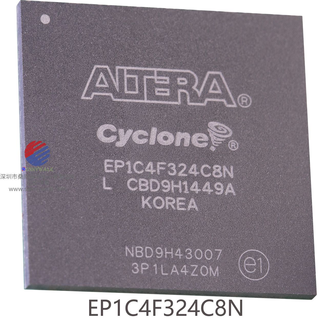
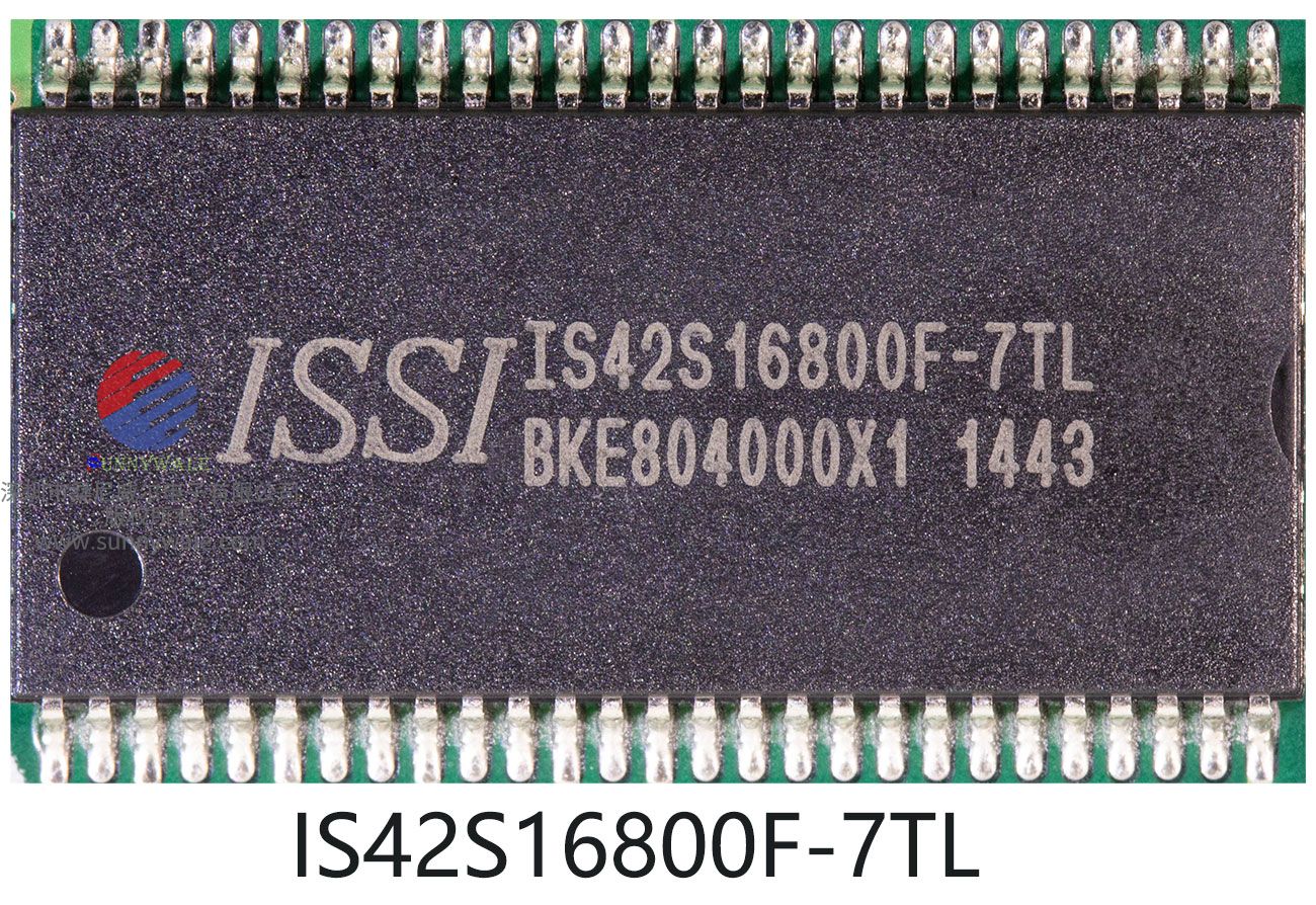
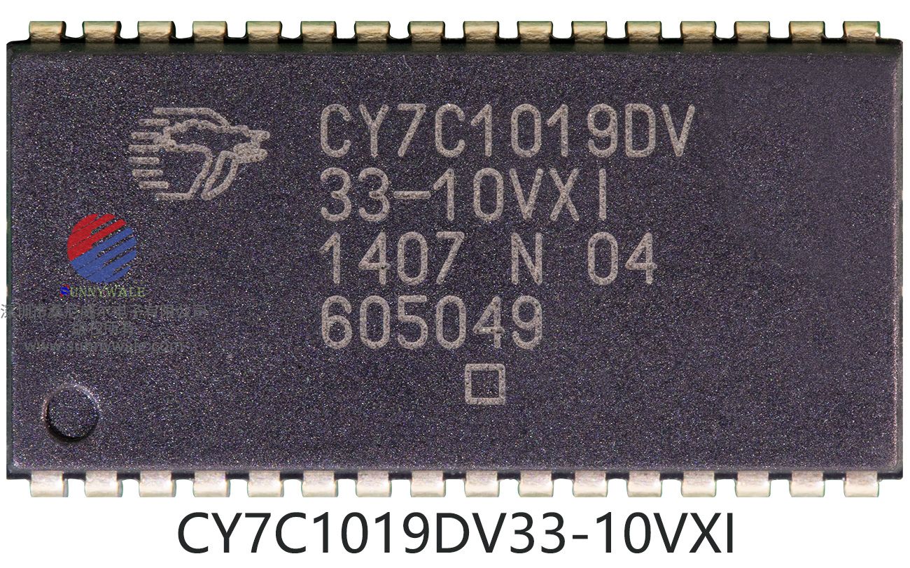
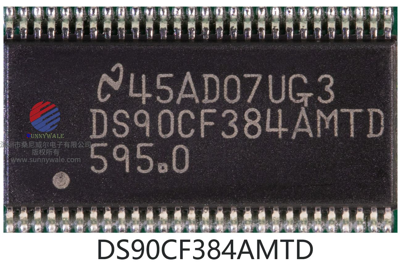
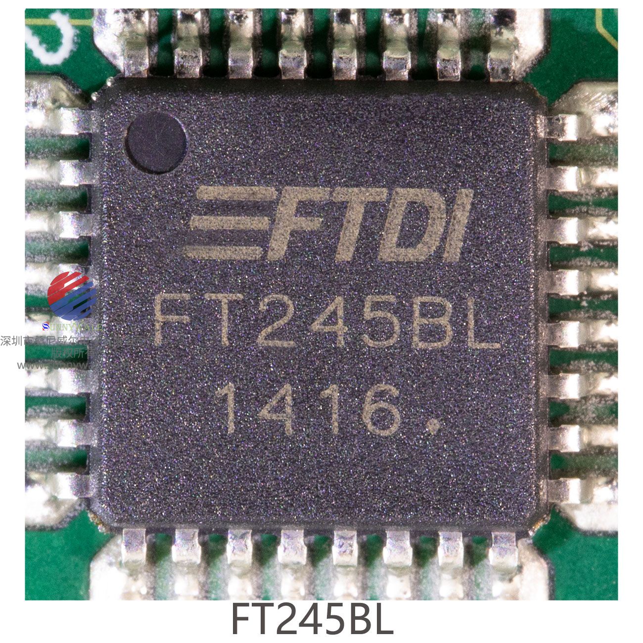
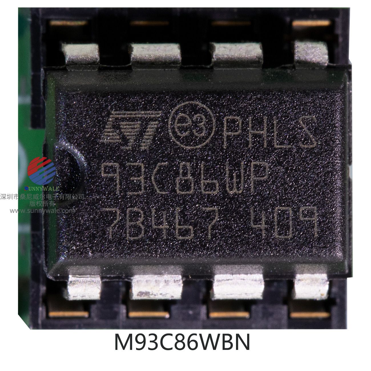
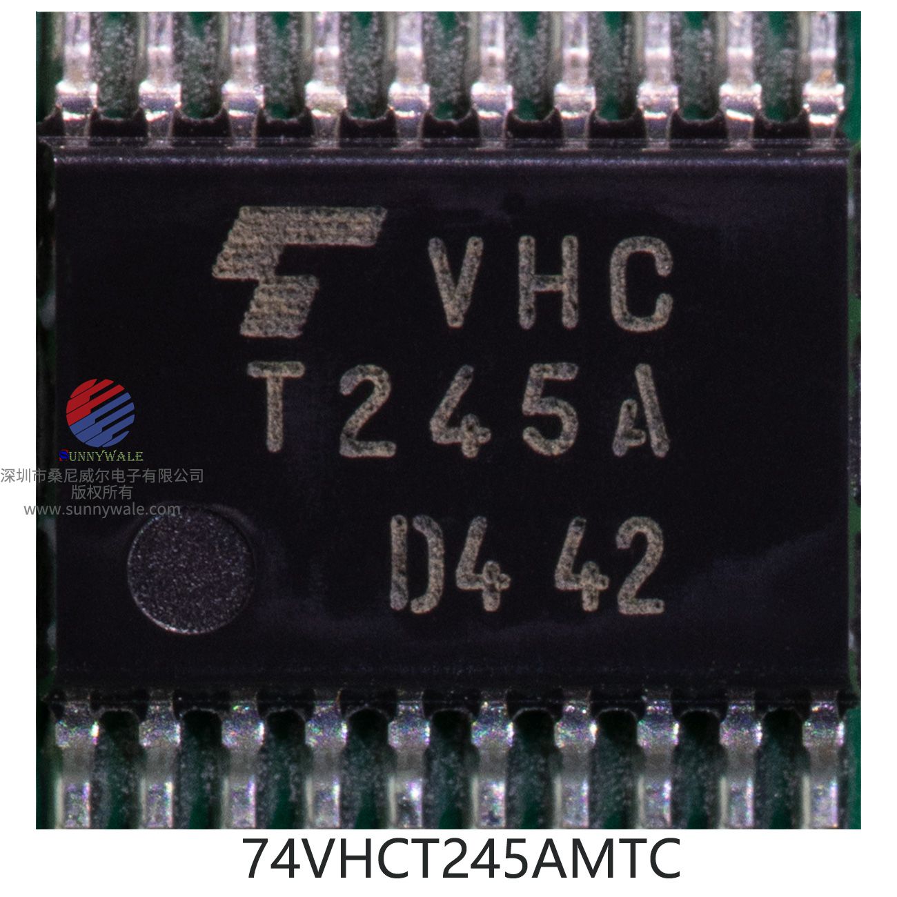
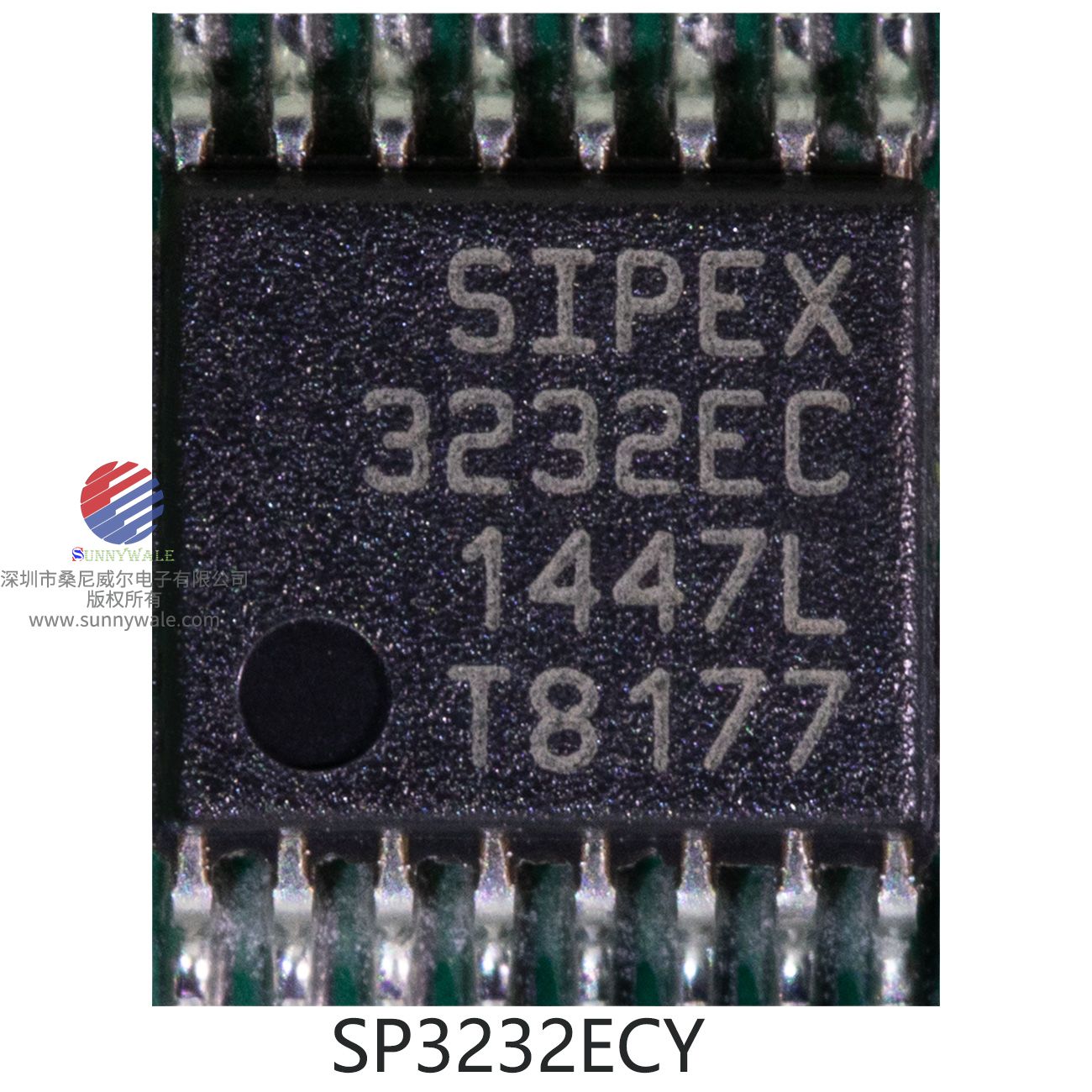
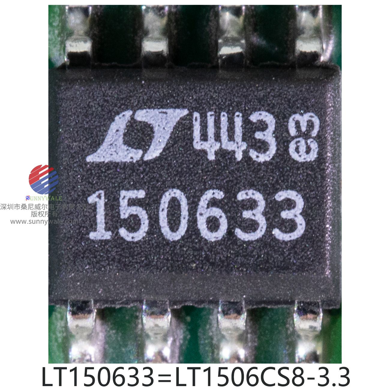
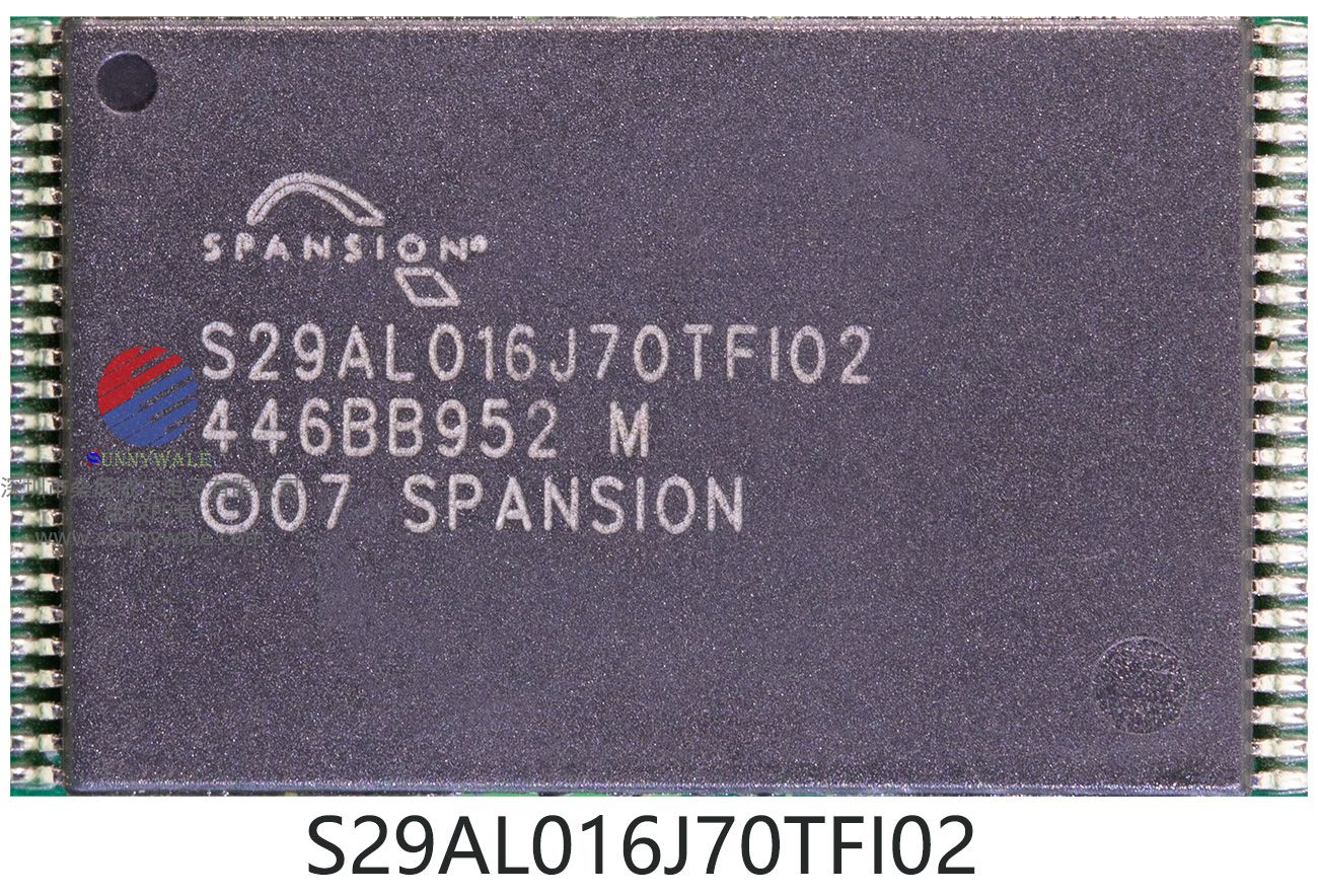
HD6417750RF200,EP1C4F324C8N,IS42S16800F-7TL,CY7C1019DV33-10VXI,DS90CF384AMTD,FT245BL,M93C86WP,74VHCT245AMTC,74VHCT244AMTC,SP3232ECY,LT1506CS8-3.3,S29AL016J70TFI02,SIPEX3232EC,VHC244=74VHCT244AMTC,VHC132=74VHC132MTC,LMV358M,ST93C46WP,45XH,X17C=ADC102S021CIMM/NOPB,LM25 BA09 BASE BOARD,DS90CF383BMT
计算机)微处理器,目标代码向上兼容SH-1、SH-2和SH3微型计算机。它包括一个指令缓存,一个可选择回拷的操作数缓存
或透写模式,以及具有64项全关联的MMU(内存管理单元)
统一TLB(翻译暂置缓冲区)。SH7750和SH7750S有一个8 kb的指令
缓存和一个16kbyte的数据缓存。SH7750R有一个16kbyte的指令缓存和一个32kbyte的指令缓存
数据缓存。
SH7750系列有一个片上总线状态控制器(BSC),允许连接到DRAM
和同步DRAM。它的16位定长指令集使程序代码的大小可以是
与32位指令相比减少了近50%。(datasheet page1)
規格
商品屬性 屬性值 選擇屬性
製造商: Intel
產品類型: FPGA - 現場可編程輯閘陣列
RoHS: 詳細資料
系列: Cyclone EPC4
邏輯元件數目: 4000 LE
自適應邏輯模組 - ALM: -
內建記憶體: 76.5 kbit
輸入/輸出數: 249 I/O
電源電壓 - 最小值: 1.5 V
電源電壓 - 最大值: 3.3 V
最低工作溫度: 0 ℃
最高工作溫度: + 70 ℃
安裝風格: SMD/SMT
封裝/外殼: FBGA-324
封裝: Tray
品牌: Intel / Altera
最大工作頻率: 250 MHz
濕度敏感: Yes
邏輯陣列區塊數目 - LAB: 400 LAB
工作電源電壓: 1.5 V to 3.3 V
產品類型: FPGA - Field Programmable Gate Array
84
子類別: Programmable Logic ICs
總記憶體: 78336 bit
公司名稱: Cyclone
零件號別名: 974157
DEVICE OVERVIEW
The 128Mb SDRAM is a high speed CMOS, dynamic random-access memory designed to operate in 3.3V Vdd and 3.3V Vddq memory systems containing 134,217,728 bits. Internally configured as a quad-bank DRAM with a synchronous interface. Each 33,554,432-bit bank is organized as 4,096 rows by 512 columns by 16 bits or 4,096 rows by 1,024 columns by 8 bits.
The 128MbSDRAM includes anAUTOREFRESH MODE, and a power-saving, power-down mode. All signals are registered on the positive edge of the clock signal, CLK. All inputs and outputs are LVTTL compatible.
The 128Mb SDRAM has the ability to synchronously burst data at a high data rate with automatic column-address generation, the ability to interleave between internal banks to hide precharge time and the capability to randomly change column addresses on each clock cycle during burst access.
A self-timed row precharge initiated at the end of the burstsequence is available with the AUTO PRECHARGE function enabled. Precharge one bank while accessing one of the other three banks will hide the precharge cycles andprovide seamless, high-speed, random-access operation.
SDRAM readandwriteaccessesareburstorientedstarting at a selected location and continuing for a programmed number of locations in a programmed sequence. The registration of an ACTIVE command begins accesses, followed by a READ or WRITE command. The ACTIVE command in conjunction with address bits registered are used to select the bank and row to be accessed (BA0, BA1 select the bank; A0-A11 select the row). The READ or WRITE commands in conjunction with address bits registered are used to select the starting column location for the burst access.
Programmable READ or WRITE burst lengths consist of 1, 2, 4 and 8 locations or full page, with a burst terminate option.
Features
- High speed:-tAA = 10 ns
- CMOS for optimum speed/power
- Center power/ground pinout
- Automatic power-down when deselected
- Easy memory expansion with CE and OE options
FEATURES
- 20 to 65 MHz Shift Clock Support
- 50% Duty Cycle on Receiver Output Clock
- Best-in-Class Set & Hold Times on RxOUTPUTs
- Rx Power Consumption <142 mW (typ) @65MHz Grayscale
- Rx Power-down Mode <200μW (max)
- ESD Rating >7 kV (HBM), >700V (EIAJ)
- Supports VGA, SVGA, XGA and Dual Pixel SXGA.
- PLL Requires no External Components
- Compatible with TIA/EIA-644 LVDS Standard
- Low Profile 56-lead or 48-lead Packages
DESCRIPTION
The DS90CF384A receiver converts the four LVDS data streams (Up to 1.8 Gbps throughput or 227 Megabytes/sec bandwidth) back into parallel 28 bits of CMOS/TTL data (24 bits of RGB and 4 bits of Hsync, Vsync, DE and CNTL). Also available is the DS90CF364A that converts the three LVDS data streams (Up to 1.3 Gbps throughput or 170 Megabytes/sec bandwidth) back into parallel 21 bits of CMOS/TTL data (18 bits of RGB and 3 bits of Hsync, Vsync and DE). Both Receivers' outputs are Falling edge strobe. A Rising edge or Falling edge strobe transmitter (DS90C383A/DS90C363A) will interoperate with a Falling edge strobe Receiver without any translation logic.
The DS90CF384A / DS90CF364A devices are enhanced over prior generation receivers and provided a wider data valid time on the receiver output.
This chipset is an ideal means to solve EMI and cable size problems associated with wide, high speed TTL interfaces.
The FT245BL is the lead free version of the 2nd generation of FTDI's popular USB FIFO IC. This device not only adds extra functionality to its FT8U245AM predecessor and reduces external component count, but also maintains a high degree of pin compatibility with the original, making it easy to upgrade or cost reduce existing designs as well as increasing the potential for using the device in new application areas.
Features
* Industry standard MICROWIRE bus
* Single supply voltage:
- 2.5 V to 5.5 V for M93Cx6-W
- 1.8 V to 5.5 V for M93Cx6-R
* Dual organization: by word (x16) or byte (x8)
* Programming instructions that work on: byte, word or entire memory
* Self-timed programming cycle with auto-erase: 5 ms
* READY/BUSY signal during programming
* 2 MHz clock rate
* Sequential read operation
* Enhanced ESD/latch-up behavior
* More than 4 million write cycles
* More than 200-year data retention
General Description
The VHCT245A is an advanced high speed CMOS octal bus transceiver fabricated with silicon gate CMOS technology. It achieves high speed operation similar to equivalent Bipolar Schottky TTL while maintaining the CMOS low power dissipation. The VHCT245A is intended for bidirectional asynchronous communication between data busses.
The direction of data transmission is determined by the level of the T/R input. The enable input can be used to disable the device so that the busses are effectively isolated.
Protection circuits ensure that 0V to 7V can be applied to the input and output (Note 1) pins without regard to the supply voltage. These circuits prevent device destruction due to mismatched supply and input/output voltages. This device can be used to interface 5V to 3V systems and two supply systems such as battery back up.
Features
■ High Speed: Tpd=5.4 ns (type) at Vcc 5V
■ Power Down Protection on Inputs and Outputs
■ Low Power Dissipation: Icc 4 μA (Max) @ TA 25°C
■ Pin and Function Compatible with 74HCT245
⑨ 74VHCT244AMTC=VHCT244(x1片):FAIRCHILD,6.5x4.4mm TSSOP20(MTC20), Octal Buffer/Line Driver with 3-STATE Outputs
Features
■ High Speed: tPD = 5.9ns (Type) at VCC = 5V
■ Power down protection is provided on inputs and outputs
■ Low power dissipation: ICC = 4μA (Max.) @ TA = 25°C
■ Pin and function compatible with 74HCT244
General Description
The VHCT244A is an advanced high speed CMOS octal bus transceiver fabricated with silicon gate CMOS technology. It achieves high speed operation similar to equivalent Bipolar Schottky TTL while maintaining the CMOS low power dissipation. The VHCT244A is a noninverting 3-STATE buffer having two active-LOW output enables. This device is designed to be used as 3-STATE memory address drivers, clock drivers, and bus oriented transmitter/receivers.
Protection circuits ensure that 0V to 7V can be applied to the input and output(1) pins without regard to the supply voltage. These circuits prevent device destruction due to mismatched supply and input/output voltages. This device can be used to interface 5V to 3V systems and two supply systems such as battery back up.
Note:1. Outputs in OFF-State
FEATURES
■ Meets true EIA/TIA-232-F Standards from a +3.0V to +5.5V power supply
■ Minimum 120Kbps Data Rate Under Full Load
■ 1μA Low-Power Shutdown with Receivers Active (SP3222E)
■ Interoperable with RS-232 down to +2.7V power source
■ Enhanced ESD Specifications:
±15kV Human Body Model
±15kV IEC1000-4-2 Air Discharge
±8kV IEC1000-4-2 Contact Discharge
DESCRIPTION
The SP3222E/3232E series is an RS-232 transceiver solution intended for portable or handheld applications such as notebook or palmtop computers. The SP3222E/3232E series has a high-efficiency, charge-pump power supply that requires only 0.1μF capacitors in 3.3V operation. This charge pump allows the SP3222E/3232E series to deliver true RS-232 performance from a single power supply ranging from +3.3V to +5.0V. The SP3222E/3232E are 2-driver/2-receiver devices. This series is ideal for portable or hand-held applications such as notebook or palmtop computers. The ESD tolerance of the SP3222E/3232E devices are over ±15kV for both Human Body Model and IEC1000-4-2 Air discharge test methods. The SP3222E device has a low-power shutdown mode where the devices' driver outputs and charge pumps are disabled. During shutdown, the supply current falls to less than 1μA.
FEATURES
■ Constant 500kHz Switching Frequency
■ Easily Synchronizable
■ Operates with Input as Low as 4V
■ Uses All Surface Mount Components
■ Inductor Size Reduced to 1.8μH
■ Saturating Switch Design: 0.07Ω
■ Shutdown Current: 20μA
■ Cycle-by-Cycle Current Limiting
APPLICATIONS
■ Portable Computers
■ Battery-Powered Systems
■ Battery Charger
■ Distributed Power
DESCRIPTION
The LT@1506 is a 500kHz monolithic buck mode switching regulator functionally identical to the LT1374 but optimized for lower input voltage applications. It will operate over a 4V to 15V input range compared with 5.5V to 25V for the LT1374. A 4.5A switch is included on the die along with all the necessary oscillator, control and logic circuitry. High switching frequency allows a considerable reduction in the size of external components. The topology is current mode for fast transient response and good loop stability. Both fixed output voltage and adjustable parts are available.
A special high speed bipolar process and new design techniques achieve high efficiency at high switching frequency. Efficiency is maintained over a wide output current range by keeping quiescent supply current to 4mA and by utilizing a supply boost capacitor to saturate the power switch.
The LT1506 fits into standard 7-pin DD and fused lead SO-8 packages. Full cycle-by-cycle short-circuit protection and thermal shutdown are provided. Standard surface mount external parts are used, including the inductor and capacitors. There is the optional function of shutdown or synchronization. A shutdown signal reduces supply current to 20μA. Synchronization allows an external logic level signal to increase the internal oscillator from 580kHz to 1MHz.
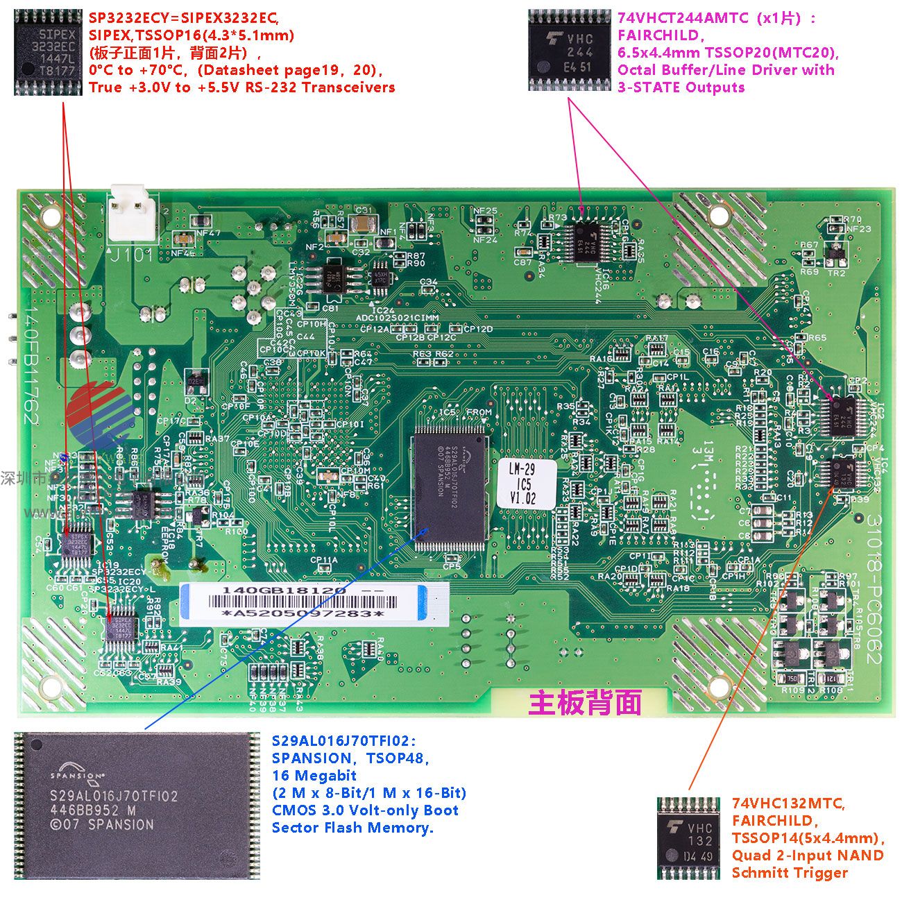
背面板载IC:
① S29AL016J70TFI02:SPANSION,TSOP48,16 Megabit (2 M x 8-Bit/1 M x 16-Bit) CMOS 3.0 Volt-only Boot Sector Flash Memory.

② SIPEX3232ECY(x 2片,正面也有) :
③ 74VHCT244AMTC=VHC244 (x2片),FAIRCHILD,6.5x4.4mm TSSOP20(MTC20),Octal Buffer/Line Driver with 3-STATE Outputs
General Description
The VHCT244A is an advanced high speed CMOS octalbus transceiver fabricated with silicon gate CMOS technol-ogy. It achieves high speed operation similar to equivalentBipolar Schottky TTL while maintaining the CMOS lowpower dissipation. The VHCT244A is intended for bidirec-tional asynchronous communication between data busses.The direction of data transmission is determined by thelevel of the T/R input. The enable input can be used to dis-able the device so that the busses are effectively isolated.
Protection circuits ensure that 0V to 7V can be applied tothe input and output (Note 1) pins without regard to thesupply voltage. These circuits prevent device destructiondue to mismatched supply and input/output voltages. Thisdevice can be used to interface 5V to 3V systems and twosupply systems such as battery back up.
Note 1: Outputs in OFF-
Features
■ High Speed: tPD 5.4 ns (typ) at VCC=5V
■ Power Down Protection on Inputs and Outputs
■ Low Power Dissipation: ICC 4 μA (Max) @ TA 25°C
■ Pin and Function Compatible with 74HCT244
④ 74VHC132MTC=VHC132:FAIRCHILD,TSSOP14(5x4.4mm),Quad 2-Input NAND Schmitt Trigger
General Description
The VHC132 is an advanced high speed CMOS 2-input NAND Schmitt Trigger Gate fabricated with silicon gate CMOS technology. It achieves the high-speed operation similar to Bipolar Schottky TTL while maintaining the CMOS low power dissipation. Pin configuration and function are the same as the VHC00 but the inputs have hysteresis between the positive-going and negative-going input thresholds, which are capable of transforming slowly changing input signals into sharply defined, jitter-free output signals. Thus greater noise margin then conventional gates is provided. An input protection circuit ensures that 0V to 7V can be applied to the input pins without regard to the supply voltage. This device can be used to interface 5V to 3V systems and two supply systems such as battery backup. This circuit prevents device destruction due to mismatched supply and input voltages.
Features
■ High Speed: tPD=3.9 ns (typ) at Vcc=5 V
■ Power down protection is provided on all inputs
■ Low power dissipation: ICC 2 μA (max) at TA 25°C
■ Low noise: Volp=0.8 V (max)
■ Pin and function compatible with 74HC132
General Description
The LMV358/324 are low voltage (2.7–5.5V) versions of thedual and quad commodity op amps, LM358/324, which cur-rently operate at 5–30V. The LMV321 is the single version.The LMV321/358/324 are the most cost effective solutionsfor the applications where low voltage operation, space sav-ing and low price are needed. They offer specifications thatmeet or exceed the familiar LM358/324.
The LMV321/358/324 have rail-to-rail output swing capability and the inputcommon-mode voltage range includes ground. They all ex-hibit excellent speed-power ratio, achieving 1MHz of band-width and 1V/μs of slew rate with low supply current.
The LMV321 is available in space saving SC70-5, which isapproximately half the size of SOT23-5. The small packagesaves space on pc boards, and enables the design of smallportable electronic devices. It also allows the designer toplace the device closer to the signal source to reduce noisepickup and increase signal integrity.
The chips are built with National’s advanced submicronsilicon-gate BiCMOS process. The LMV321/358/324 havebipolar input and output stages for improved noise perfor-mance and higher output current drive.
Features
(For V+= 5V and V-= 0V, Typical Unless Otherwise Noted)
■ Guaranteed 2.7V and 5V Performance
■ No Crossover Distortion
■ Space Saving Package:SC70-5 2.0x2.1x1.0mm
■ Industrial Temp. Range:-40 °C to +85 °C
■ Gain-Bandwidth Product: 1MHz
■ Low Supply Current
- LMV321:130μA
- LMV358:210μA
- LMV324:410μA
■ Rail-to-Rail Output Swing@10k Ohm :
V+:-10mV ,
V-: +65mV
■ VCM:-0.2V to V+ -0.8V
Applications
■ Active Filters
■ General Purpose Low Voltage Applications
■ General Purpose Portable Devices
⑦ ADC102S021CIMM/NOPB=X17C :TI,VSSOP8, 2 Channel, 50 ksps to 200 ksps, 10-Bit A/D Converter
FEATURES
■ No Special Start-up Sequence Required Between Clock/Data and /PD Pins. Input Signal (Clock and Data) Can be Applied Either Before or After the Device is Powered.
■ Support Spread Spectrum Clocking Up to 100KHz Frequency Modulation & Deviations of ±2.5% Center Spread or-5% Down Spread."
■ Input Clock Detection" Feature Will Pull All LVDS Pairs to Logic Low when Input Clock is Missing and When /PD Pin is Logic High.
■ 18 to 68 MHz Shift Clock Support
■ Best-in-Class Set & Hold Times on TxINPUTs Tx Power Consumption < 130 mW (typ) @65MHz Grayscale
■ 40% Less Power Dissipation Than BiCMOS Alternatives
■ Tx Power-down Mode < 60μW (typ)
■ Supports VGA, SVGA, XGA and Dual Pixel SXGA.
■ Narrow Cus Reduces Cable Size and Cost
■ Up to 1.8 Gbps Throughput ■ Up to 227 Megabytes/sec Bandwidth
■ 345 mV (typ) Swing LVDS Devices for Low EMI
■ PLL Requires No External Components Compatible with TIA/EIA-644 LVDS Standard
■ Low Profile 56-Lead TSSOP Package
■ Improved Replacement for:SN75LVDS83, DS90CF383A
DESCRIPTION
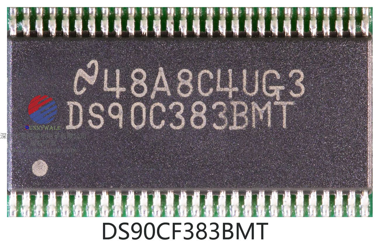
The DS90CF383B transmitter converts 28 bits of CMOS/TTL data into four LVDS (Low Voltage DffrntalSignaling)data streams.A phase-locked transmit clock is transmitted in parallel with the data streams over a fifth LVDS link. Every cycle of the transmit clock 28 bits of input data are sampled and transmitted. At a transmit clock frequency of 65 MHz, 24 bits of RGB data and 3 bits of LCD timing and control data (FPLINE, FPFRAME, DRDY) are transmitted at a rate of 455 Mbps per LVDS data channel. Using a 65 MHz clock, the data throughput is 227 Mbytes/sec. The DS90CF383B is fixed as a Falling edge strobe transmitter and will interoperate with a Falling edge strobe Receiver (DS90CF386) without any translation logic.
This chipset is an ideal means to solve EMI and cable size problems associated with wide, high speed TTL interfaces.
